B. Sensor Design and Development History
The Tunneling Infrared Sensor (TIS) was designed and developed by Stanford Professor Tom Kenny and colleagues of his at the Center for Space Microelectronics Technology at the Jet Propulsion Laboratory (JPL). The driving technological motivation for the sensor development was to create miniature sensors with high performance. Due to recent technical advances in silicon micromachining, JPL investigated a series of micromachined displacement transducers based upon the electron tunneling phenomena. Electron tunneling is a quantum mechanical phenomena originally developed for use in microscopy. The advantage of this type of transducer is that it can be miniaturized without loss in performance.
Tunneling Infrared Sensor and Principles of Operation
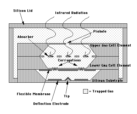
As illustrated in the Figure below, the design of the TIS is based on a thermopneumatic process that involves detecting the thermal expansion of a gas filled chamber. As shown, the sensor consists of an absorbing element suspended within a small chamber of gas. Incident infrared radiation passes through a window and irradiates a thin Pt metal absorber. The absorber heats up, and by conduction increases the temperature of the trapped gas. This increase in temperature of the gas results in increased pressure within the chamber. The increased pressure creates a force exerted on the flexible membrane walls of the chamber. The deflection of this membrane is detected by a tunneling displacement transducer, which measures variations in the quantum mechanical tunneling current between the moving membrane and the fixed tip. Because tunneling only occurs when the tip electrode is within 1 nm of the membrane electrode, the gap between the electrodes must be controlled by feedback during operation. This is accomplished by measuring the tunneling current, comparing it to a reference value, and applying correction signals to an electrostatic actuator. The actuator consists of a deflection electrode that applies rebalance forces to the moving membrane element to keep the tip-element gap constant (force-rebalance position control). If the gain of the transducer, circuit, and actuator is sufficient, the tunneling current, and therefore the gap will be maintained in the presence of external disturbances. By measuring the feedback signals required to control the position of the membrane, the amount of infrared radiation incident upon the sensor can be determined. To minimize the effect of several possible noise sources (such as slowly changing ambient temperature) a 0.5 µm diameter pinhole in the upper membrane was created and the sensor was hermetically sealed with a silicon lid (as shown in Figures below). This pinhole allows the pressure in the trapped gas to equilibrate with a larger volume of surrounding gas within a time period that is acceptably short (e.g. 2 - 10 s), yet long enough to permit detection of radiation induced signals at frequencies > 1 Hz.
TIS Design
(for better picutes and more information on the TIS click here.)
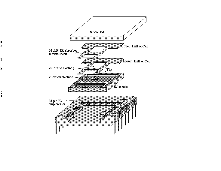
The TIS is created by using silicon micromachining techniques to fabricate the individual components of the sensor. After the fabrication of these individual sensor components, the sensors are individually assembled by hand using a four step process. The first step consists of mounting a substrate element into a standard 28 pin IC style chip carrier package with rapid-curing epoxy. Gold wire bond connections between the electrodes and the IC. Next, the upper and lower membranes are bonded together to create the internal gas cell. Step 3 consists of aligning and bonding the gas cell structure formed in step 2 to the substrate carrier structure created in step 1. The final step involves epoxying the silicon lid on top of the 28 pin IC sensor package to hermetically seal the entire package. A large quantity (>100) sensors have been successfully assembled in this manner. An exploded view of the individual TIS components is shown in the Figure below.
Sensor Performance
The sensor may be operated with simple feedback circuitry, and exhibits remarkable sensitivity and bandwidth. A laser interferometer independently measured the actual transducer responsivity to be 80 Angstroms/V, which results in a displacement resolution of 0.007 Angstroms per root Hz at 10 Hz. In addition, a calibrated responsivity measurement was made on the TIS using a NIST-traceable calibrated blackbody infrared source heated to 800 C and a narrowband infrared filter. Using a HP3582B spectrum analyzer, the TIS sensor NEP was measured to be 3 E-10 W per root Hz at 25 Hz.
Based on these results, the TIS performance is competitive with the state of the art for mm-sized uncooled infrared sensors. In addition, these sensors are easily operated, and are extremely robust. These features indicate that the TIS might be ideally suited for space-based measurement of long-wave thermal infrared radiation from planetary surfaces. Potential applications for the TIS include its use in Earth horizon detectors and planetary thermal mapping instruments. In addition, it is expected that several other commercial and NASA space applications exist which can be expected to benefit from the use of this new sensor technology.
Back to THD Summary