ALD-Enhanced Bolometer
The goal of this project is to develop bolometer arrays using a metal thin film formed by atomic layer deposition (ALD). Nanometer-thick freestanding layers deposited by ALD process have the potential to improve the performance of bolometers with achieving low thermal conductance and optimal optical properties.
A bolometer is a device to measure the energy of incident infrared radiation with resistance change. This device is widely used for the thermal imaging applications such as night vision. A standard bolometer consists of a thermally isolated freestanding membrane, supporting beams, and a thermistor (Fig. 1). The absorption of incoming infrared radiation in the membrane increases the temperature of the device. This temperature change is measured by the resistance change of the thermistor. The improvement of the bolometersÅf performance can be achieved by minimizing the thermal conductance of the suspended structure, maximizing the absorption coefficient, and maximizing the ratio of the TCR to the normalized 1/f noise. Conventional bolometers consist of multiple functional layers to optimize their performance. These functional layers can be replaced by one metal layer to further reduce the thermal conductance and simplify the fabrication process. However, this requires a film thickness in the order of nanometers since the impedance of the film must approach that of free space in order to absorb the wavelengths of the interest (8-14 um). We propose an uncooled infrared bolometer using a few-nanometer-thick metal film that is formed by ALD. ALD is used to reliably deposit metal films with less than 10-nm thickness. The ALD metal film is used both as the absorber and as supporting beams. The thermal capacitance is greatly reduced since the membrane is much thinner than the conventional dielectric absorbers. Therefore, the thermal insulation can be further improved while keeping the thermal time constant at an acceptable value. The fist implementation of the proposed bolometer is fabricated and characterized. Fig. 2 shows SEM image of the fabricated device. The device is made by about 14-nm Al2O3/Pt stack that are formed by ALD. The dimensions of the freestanding membrane is 50x50 um. Currently, we are working on the chracterization of the devices and the fabrication of bolometer arrays using surface micromachining. For further information, please check related publications or contact us.
Related Publications:
- S. Yoneoka, M. Liger, G. Yama, R. Schuster, F. Purkl, J Provine, F. B. Prinz, R. T. Howe, and T. W. Kenny, "ALD-metal uncooled bolometer," Proc. 24th IEEE MEMS 2011, Cancun, Mexico, 2011, Accepted.
Contact Information:
Address: Bldg. 530, Room 224, 440 Escondido Mall, Stanford, CA 94305
Email: yoneoka AT stanford DOT edu
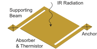 |
Figure 1: Schematic of a standard bolometer |
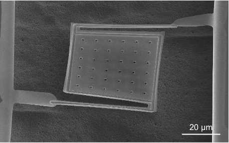 |
Figure 2: SEM image of the fabricated bolometer |