MEMS Inertial Sensors in Epi-seal
Ian B. Flader, Yunhan Chen
Summary - Epi-seal is a hermetic, wafer-encapsulation MEMS process which provides a platform for the fabrication of ultra-stable, high quality factor MEMS resonators. Stability and quality factor are important parameters for devices which require high levels of frequency stability, such as timing references. Inertial sensors also benefit from these inherent qualities, however they are difficult to successfully fabricate due to the encapsulation process. Recently, our lab has developed new fabrication and design techniques which address the issues related to fabrication of inertial sensors in Epi-seal.
Fully Differential Electrodes
Differential drive and sense configurations are paramount for MEMS transduction. Differential readouts will reject common sources of noise, i.e. common-mode rejection ratio (CMRR). Differential configurations can also be used to reject certain resonant modes while amplifying resonant modes of interest. One in-plane (IP) resonant mode with differential configuration is sufficient for many time keeping applications. However, for inertial sensors (especially multi-axis sensors) differential readouts for both in-plane and out-of-plane (OOP) modes are beneficial. Figure 1 shows the fabrication process developed to incorporate these features inside a wafer-encapsulation.
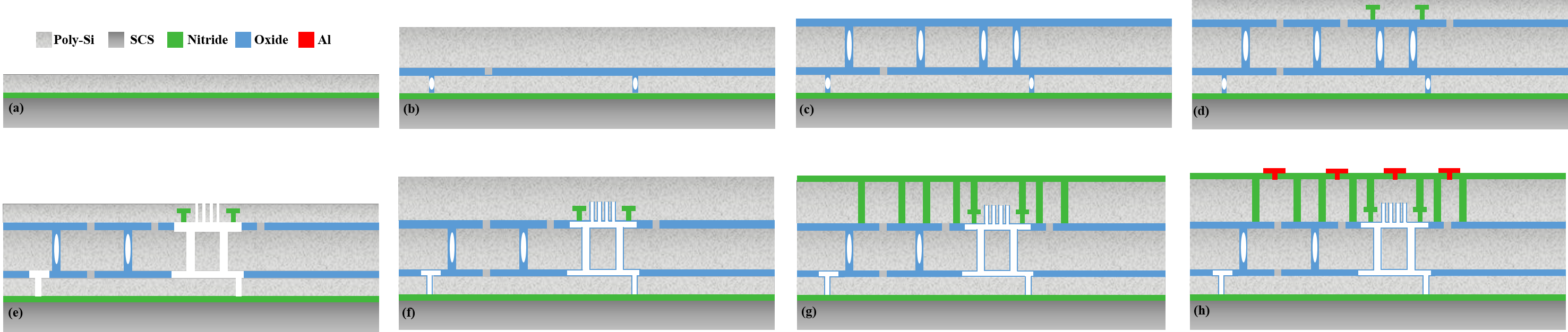
Figure 1. Schematic of fabrication process flow. Oxide coated polysilicon devices were fabricated inside a wafer encapsulation. Bottom electrode, device, and top electrode layers were deposited inside an epitaxial silicon reactor.
While differential configurations can be achieved for in-plane resonant modes of standard Epi-seal devices, a new fabrication process had to be developed to achieve the same for out-of-plane resonant modes. To achieve this, bottom and top electrodes had to be integrated with the standard Epi-seal process. This was done by growing each silicon layer (bottom, device, top) in an epitaxial silicon furnace. Figure 2 shows fabrication details at various stages of the process.
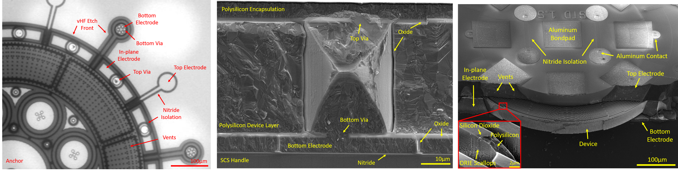
Figure 2. (left) Top-view infrared image of device after releasing of sacrificial oxide. (middle) SEM before HF release showing electrical vias from the top encapsulation layer to the bottom electrode. (right) SEM of fabricated disk resonant gyroscope (DRG) showing the thin oxide coating around the polysilicon device.
Electrical connection to the bottom, device, and top layers provided by this new process allow for the fully differential driving and sensing of both in-plane and out-of-plane resonant modes while maintaining the hermeticity of the standard process. Figure 3 shows the frequency response for devices fabricated in the new process. Identical devices were fabricated in single crystal silicon (standard process) and oxide-coated polysilicon to demonstrate the conservation of the standard Epi-seal merits.
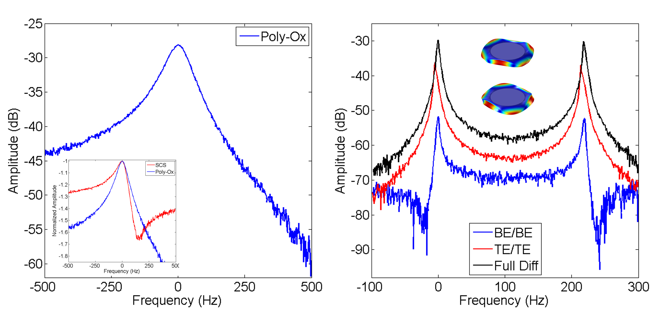
Figure 3. Open loop frequency responses of a (left) DETF and (right) DRG. The DRG was driven with pairs of bottom (BE) and top (TE) electrodes for differential and non-differential transduction of the OOP mode.
Large Transduction Gaps
Another limitation regarding the standard Epi-seal process is the fixed range (0.7 - 1.5um) for lateral transduction gaps. This range is defined by the maximum Deep Reactive Ion Etch (DRIE) trench width which can be filled by tetraethyl orthosilicate (TEOS) oxide and the minimum size feature which can be defined lithographically. Previous attempts have been successful in removing this restriction by the use of wafer bonding. However, wafer bonding can introduce many fabrication defects caused by a number of sources such as wafer roughness, bow, particle contaminants, and planarization.
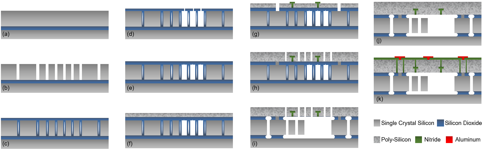
Figure 4. Process flow utilizing XeF2 to achieve large transduction gaps.
To bypass issues related to wafer bonding we developed a new Epi-seal fabrication process which utilizes vapor phase xenon difluoride (XeF2) to create large transduction gaps using a single silicon on insulator (SOI) wafer. This is done by defining sacrificial silicon areas using DRIE which are subsequently etched using XeF2. TEOS oxide is used as an etch stop during this process and is later etched during the vapor phase hydrofluoric acid releasing step. Figure 4 summarizes the fabrication process.
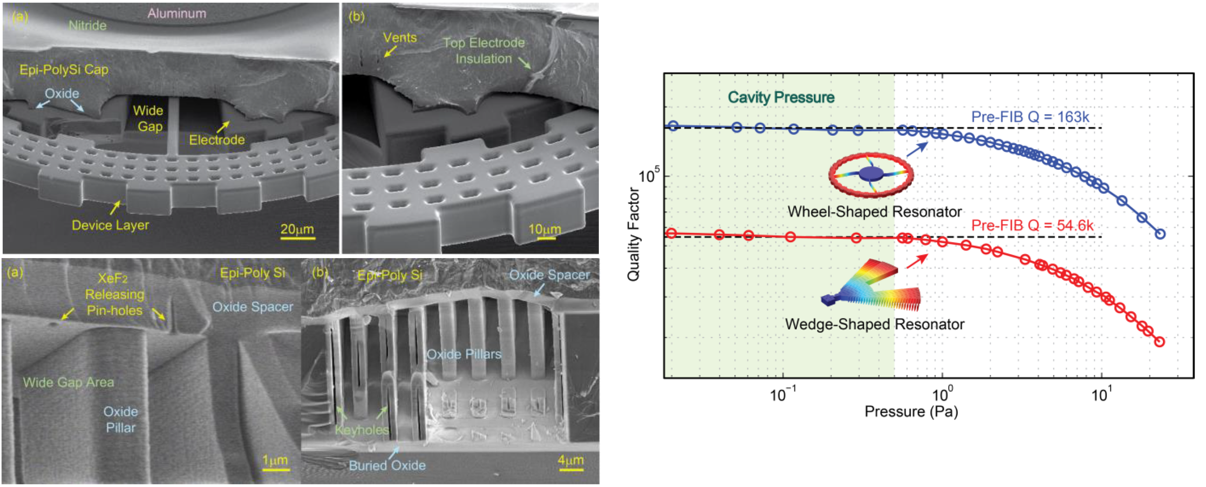
Figure 5. SEM images of fabricated devices. (top, left) Fabricated wheel resonator. (bottom, left) Oxide support pillars before sacrificial oxide etch. (right) Pressure sweep showing encapsulated, near-vacuum operation pressure.
SEM images were taken of the fabricated devices in Figure 5. Shown in the SEMs is a fabricated wheel resonator with ~40um lateral transdcution gap. The oxide support pillars which serve as mechanical support for the encapsulation as well as an etch barrier during the XeF2 etch are shown as well. The pressure sweep shown in Figure 5 demonstrates that the high vacuum and hermeticity characteristic of Epi-seal is preserved for the fabrication process. This makes the process well suited for many MEMS applications
Combined Process
The two processes described above were integrated together to create bare polysilicon devices with bottom, top, and in-plane electrodes along with large transduction gap capabilities. The integrated process allows for the fabrication of MEMS inertial sensors with differential in-plane and out-of-plane transduction as well as large inertial deflections. In addition, this process allows for the study of fatigue mechanisms in bare, oxide-free polysilicon inside a hermetic environment for the first time, as well as resonator dynamics in a strongly nonlinear regime.
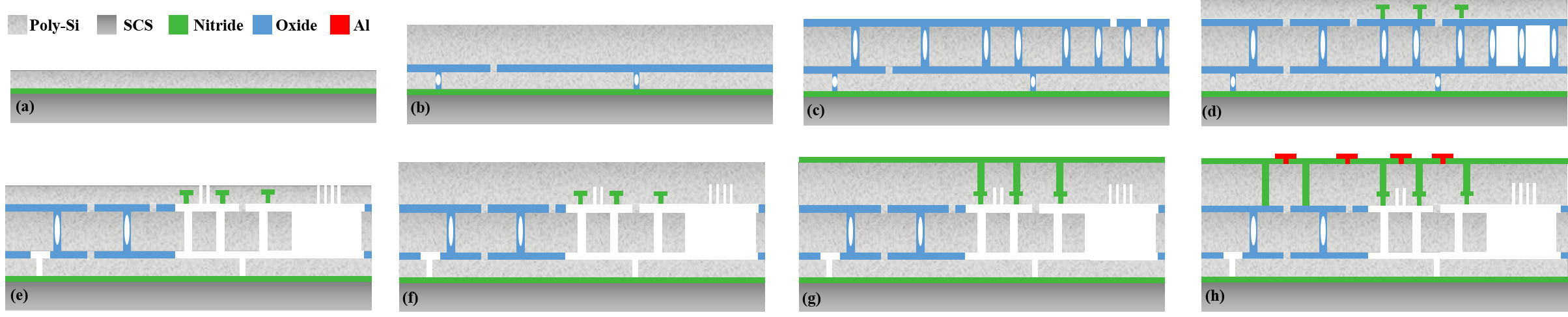
Figure 6. Fabrication process for integration of differential out-of-plane electrodes and large lateral transduction gaps.
Figure 6 summarizes the fabrication process. Fabrication begins with a SCS wafer and each conducting layer (bottom, device, top) is grown in an epitaxial reactor. The polysilicon layers were etched using DRIE and TEOS oxide was used as a spacer between the conducting layers. Vapor phase XeF2 was used to etch designated areas of sacrificial silicon, while vHF was used to etch the sacrificial TEOS oxide.
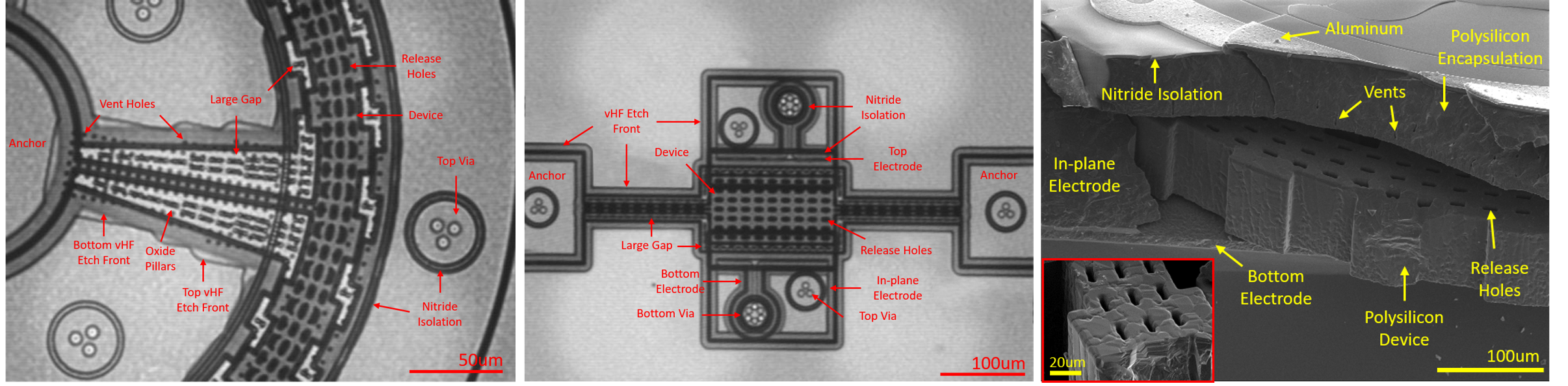
Figure 7. (left) IR image of wheel resonator demonstrating large lateral transduction gaps. (middle) IR image of a fringe actuated resonator utilizing differential out-of-plane electrodes. (right) SEM of a fabricated wheel resonator with various encapsulation features visible.
Figure 7 shows infrared images taken immediately after the vHF etch of TEOS oxide. Shown in the figure are locations where large lateral transduction gaps have been created as well as the functional features created to achieve electrodes underneath the device layer. SEMs of the fabricated devices were also taken and shown in Figure 7. The SEM shows the encapsulated wheel resonator with bottom, top, and in-plane electrodes. Additionally, the expected roughening of the polysilicon grains during the high temperature sealing phase is shown in the inset of Figure 7.
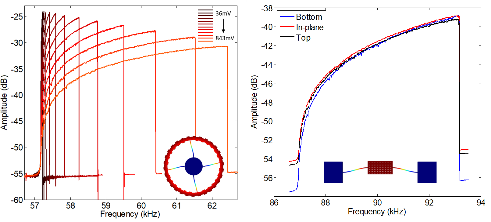
Figure 8. Frequency response measurements of (left) wheel resonator and (right) fringe actuated resonator in the strongly nonlinear regime.
Due to the large transduction gaps and multi-layer electrodes enabled by this fabrication process, it was possible to drive devices into a strongly nonlinear regime (Figure 8). A wheel resonator with large lateral gaps was driven with excitation voltages ranging from 36mV to 843mV into a strongly nonlinear regime. Additionally, the nonlinear response of a fringe actuated device is shown using bottom, top, and in-plane electrodes independently.
Micro-tethering
The fabrication processes above address many performance and functional limitations for inertial sensors inside the Epi-seal process. However, sensors requiring large released areas for inertial proof masses are still susceptible to stiction related failures during fabrication. Micro-tethering is a technique developed to temporarily increase the device rigidity during fabrication. Silicon tethers are created during the fabrication of devices to hold compliant structures in place to additional anchor supports. These tethers are later removed after successful fabrication to achieve high sensitivity operation.
Figure 9. (right) Schematic showing the tethered resonant accelerometer. (top, left) SEM image of the tethered device. (bottom, left) X-ray image of fabricated device demonstrating stiction of the proof mass to the wafer substrate.
Tethers were added to compliant devices and removed after successful fabrication by either joule melting of the silicon tether or shear fracturing. The tethers were designed to have the highest joule heating along the tether beam, and a heating current was supplied to the device until successful detachment. Additionally, devices were designed to separate under large enough external impacts by mechanical shearing.
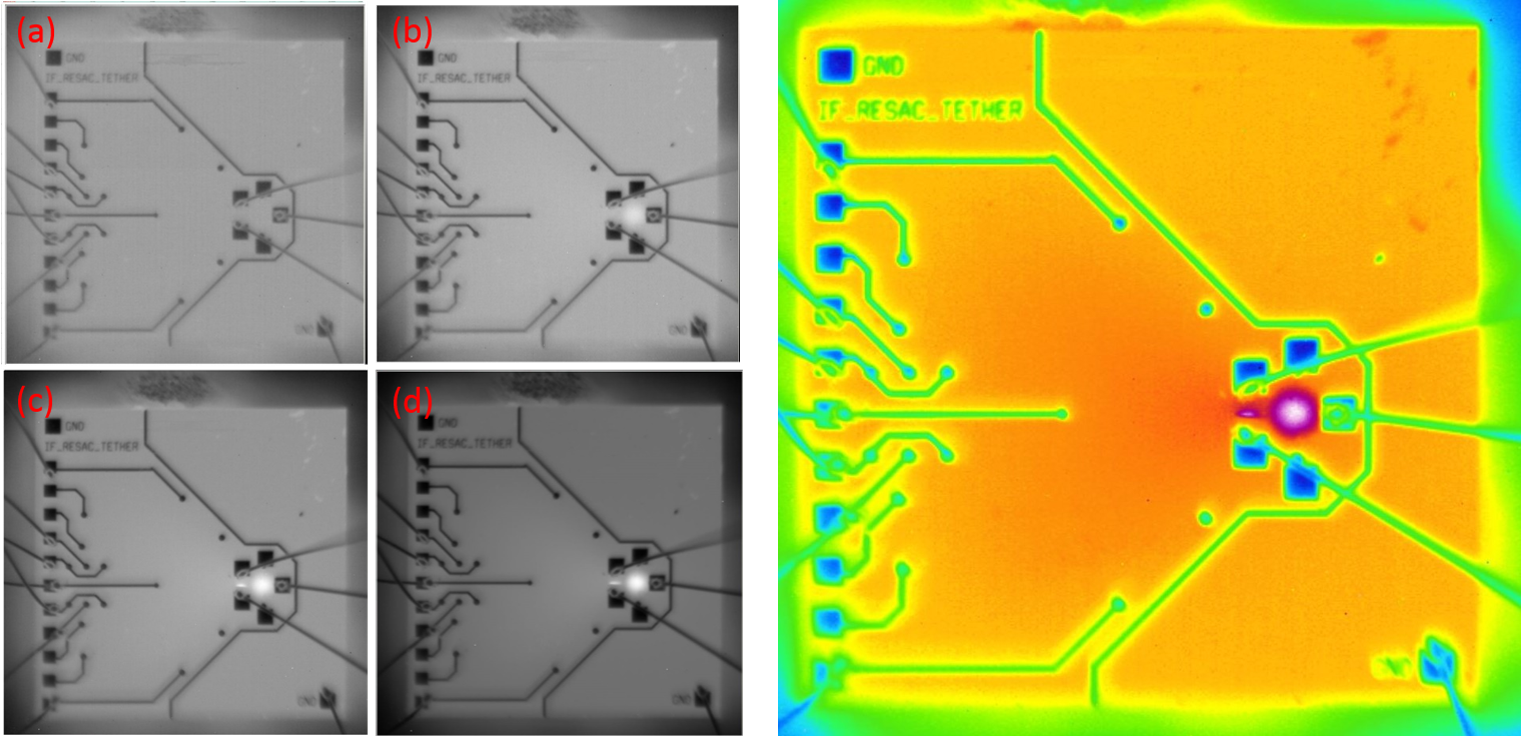
Figure 10. IR images of joule heated devices. (left) Infrared with increasing heating currents from (a) 0mA to (d) 70mA. After application of 70mA of heating current the tether separated and current was no longer able to flow. (right) Emissivity of heated silicon.
Devices were heated by applying a potential difference across two voltage terminals. Infrared images were taken in Figure 10 and it was shown that joule heating was concentrated in the device tethers as intended. In this way devices could be heated until detachment of the temporary tether for high sensitivity operation.
Table 1. Performance Summary Before and After Tether Detachment for Various Methods.

Device tethers were designed to detach by two methods: joule heating and mechanical fracture. The accelerometers were characterized before and after detachment and their results are shown in Table 1. As expected, device sensitivity to acceleration increased after detachment of the inertial proof mass for the two methods. In addition, it was observed that some accelerometers were detached without any additional effort post-fabrication. It was determined that some devices underwent large enough impacts during fabrication to release the inertial proof mass after the critical stiction steps where identical accelerometers without tethers failed.
Conclusion
Epi-seal is a remarkable MEMS fabrication technology which enables extremely robust and high performance MEMS resonators. This process has been leveraged with much success for applications in miniaturized time keeping references and clocks. The merits of Epi-seal are promising for applications in the field of miniaturized, high performance inertial sensors. However, key limitations prevent the process from direct application. Our work has tackled these key limitations and provided methods for robust fabrication.
[1] Ian B. Flader, Yunhan Chen, Dustin D. Gerrard, and Thomas W. Kenny, "Wafer-scale Encapsulation of Fully Differential Electrodes for Mutli-axis Inertial Sensing," 2017 19th International Conference on Solid-State Sensors, Actuators and Microsystems (TRANSDUCERS), pp. 591-594, Jun 2017. [2] Yunhan Chen, Ian B. Flader, Dongsuk D. Shin, Chae Hyuck Ahn, Janna Rodriguez, and Thomas W. Kenny, "Robust Method of Fabricating Epitaxially Encapsulated MEMS Devices with Large Gaps," Journal of Microelectromechanical Systems, Vol. 26, No. 6, pp. 1235-1243, Dec 2017. [3] Yunhan Chen, Ian B. Flader, Dongsuk D. Shin, Chae Hyuck Ahn, Lizmarie Comenencia Ortiz, Thomas W. Kenny, "Fabrication of Wide and Deep Cavities for Silicon MEMS Devices without Wafer Bonding," Journal of Microelectromechanical Systems, Vol. 26, No. 6, pp. 1235-1243, Dec 2017. [4] Ian B. Flader, Yunhan Chen, Chae Hyuck Ahn, Dongsuk D. Shin, Anne L. Alter, Janna Rodriguez, and Thomas W. Kenny, "Epitaxial Encapsulation of Fully Differential Electrodes and Large Transduction Gaps for MEMS Resonant Structures," MEMS 2018, Belfast, Northern Ireland, UK, January 21-25, 2018 [5] Ian B. Flader, Yunhan Chen, Dongsuk D. Shin, David B. Heinz, Lizmarie Comenencia Ortiz, Anne L. Alter, Woosung Park, Kenneth E. Goodson, and Thomas W. Kenny, "Micro-tethering for in-process Stiction Mitigation of Highly Compliant Structures," MEMS 2017, Las Vegas, NV, USA, January 22-26, 2017.